Ultrafast Semiconductor Chip Bonding Using Intense Pulsed Light Soldering for Chip-on-Glass Packaging
By Taejoon Noh 1, Eun-Chae Noh 2, Minjae Sung 1, Jaejun Yoon 1, Ho-Kyeong Seong 1, Dong-Gil Kang 1, Jeong-Won Yoon 2, Seung-Boo Jung 1
1 Sungkyunkwan University, Suwon, Gyeonggi-do 16419, Republic of Korea
2 Chungbuk National University, Cheongju, Chungbuk 28644, Republic of Korea
Abstract
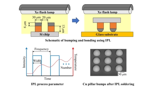
The increasing demand for miniaturization and improved performance in electronic devices has driven the exploration of glass substrates and advanced soldering techniques. Intense pulsed light (IPL) soldering with rapid heating capability presents a promising alternative to conventional reflow soldering, particularly for thermally sensitive substrates such as glass. However, despite the advantages of localized and low thermal budget processing of IPL soldering, its applicability to fine-pitch Cu pillar bump joints on glass substrates has not been thoroughly investigated. This study was aimed at examining the application of IPL soldering for Sn–2.5Ag solder-capped Cu pillar bump joints on glass substrates. Si dies with Cu pillar bumps (30 μm diameter, 50 μm pitch) were prepared, and glass substrates incorporating Kelvin structures were used for measuring the interconnection resistance. IPL soldering was compared to conventional reflow soldering in terms of electrical performance. Microstructural analysis using SEM and FIB revealed that compared with reflow soldering, IPL soldering produced thinner intermetallic compound layers, enhancing the joint reliability. Electrical resistance measurements indicated that interconnection resistance decreased with increasing IPL irradiation counts as the solder fully melted and formed stable joints, reaching the optimal value at 50–60 irradiations. These findings establish IPL technology as a promising method for soldering Cu pillar bumps onto glass substrates, offering reduced energy consumption and thermal stress, improved metallurgical reliability, and enhanced electrical performance compared with traditional reflow methods. Therefore, it is expected to emerge as a next-generation bonding technology that forms stable joints in advanced semiconductor packages.
To read the full article, click here
Related Chiplet
- DPIQ Tx PICs
- IMDD Tx PICs
- Near-Packaged Optics (NPO) Chiplet Solution
- High Performance Droplet
- Interconnect Chiplet
Related Technical Papers
- Thermal stability enhancement of low temperature Cu-Cu bonding using metal passivation technology for advanced electronic packaging
- Die-Level Transformation of 2D Shuttle Chips into 3D-IC for Advanced Rapid Prototyping using Meta Bonding
- Ammonia Plasma Surface Treatment for Enhanced Cu–Cu Bonding Reliability for Advanced Packaging Interconnection
- Material Needs and Measurement Challenges for Advanced Semiconductor Packaging: Understanding the Soft Side of Science
Latest Technical Papers
- Affinity Tailor: Dynamic Locality-Aware Scheduling at Scale
- AMMA: A Multi-Chiplet Memory-Centric Architecture for Low-Latency 1M Context Attention Serving
- Exploring the Efficiency of 3D-Stacked AI Chip Architecture for LLM Inference with Voxel
- Epoxy Composites Reinforced with Long Al₂O₃ Nanowires for Enhanced Thermal Management in Advanced Semiconductor Packaging
- Chipmunq: A Fault-Tolerant Compiler for Chiplet Quantum Architectures