TSMC looks to standardise chiplet protocols in "world changing" move
By Nick Flaherty, eeNews Europe (October 9, 2023)
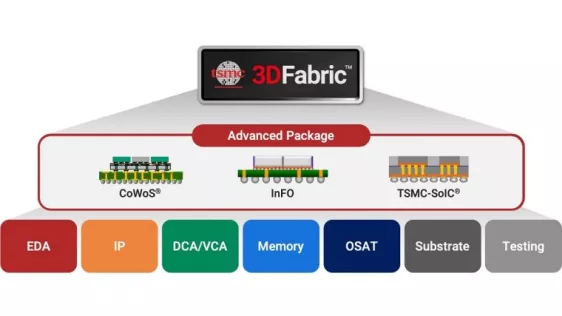
TSMC is looking to develop a standard data format for chiplet designs that would be used by all the EDA design tool and assembly and test providers.
This is part of a move to the 3D Blox technology for building chiplet designs on the TSMC CoWoS process. The aim is to provide common data for chiplets from different silicon suppliers, substrate and PCB makers and the OSAT assembly and test companies.
“Today most of the chips except for the memories come from TSMC but the goal is to mix and match but that is still some way to go but we are trying to get there,” said Dan Kochpatcharin, head of Design Infrastructure at TSMC.
To read the full article, click here
Related Chiplet
- DPIQ Tx PICs
- IMDD Tx PICs
- Near-Packaged Optics (NPO) Chiplet Solution
- High Performance Droplet
- Interconnect Chiplet
Related News
- Alphawave Semi Taped-Out Industry Leading 64Gbps UCIe™ IP on TSMC 3nm for the IP Ecosystem, Unleashing Next Generation of AI Chiplet Connectivity
- Alphawave Semi Delivers Cutting-Edge UCIe™ Chiplet IP on TSMC 3DFabric® Platform
- Strategic alignment between imec and Japan’s ASRA aims to harmonize standardization of automotive chiplet architectures
- Socionext Announces Collaboration with Arm and TSMC on 2nm Multi-Core Leading CPU Chiplet Development
Latest News
- Xanadu and EV Group partner to build industrial-scale photonic quantum hardware
- AI Optical Interconnect Boom Drives U.S. Firms to Expand Southeast Asia Outsourcing, Opening the Door for Cross-Industry Entrants
- GlobalFoundries accelerates adoption of co-packaged optics for advanced AI data centers with SCALE optical module solution
- TSMC SoIC roadmap targets 2029 chip stacking
- Applied Materials Broadens Advanced Packaging Portfolio with Acquisition of NEXX