TSMC SoIC roadmap targets 2029 chip stacking
By Brian Tristam Williams, eeNews Europe | April 29, 2026
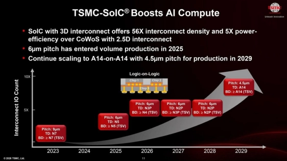
TSMC is pushing its 3D chip-stacking roadmap towards finer interconnect pitches and tighter integration as advanced packaging becomes a larger part of performance scaling for AI and high-performance computing designs.
The updated TSMC SoIC roadmap, reported after the company’s 2026 North America Technology Symposium in Santa Clara, points from 6 µm pitches today towards 4.5 µm by 2029. That direction matters because pitch scaling in hybrid-bonded die stacks directly affects the number of vertical interconnects that can be placed between chiplets.
TSMC separately said at its 2026 North America Technology Symposium that A14-to-A14 SoIC is set to be available for production in 2029, providing 1.8x higher die-to-die I/O density than N2-on-N2 SoIC. The company positions the technology as part of its wider 3DFabric advanced packaging family, alongside CoWoS and InFO.
To read the full article, click here
Related Chiplet
- DPIQ Tx PICs
- IMDD Tx PICs
- Near-Packaged Optics (NPO) Chiplet Solution
- High Performance Droplet
- Interconnect Chiplet
Related News
- Optimizing Wafer Edge Processes For Chip Stacking
- Synopsys and TSMC Pave the Path for Trillion-Transistor AI and Multi-Die Chip Design
- Cadence and TSMC Advance AI and 3D-IC Chip Design with Certified Design Solutions for TSMC’s A16 and N2P Process Technologies
- GUC Tapes Out Industry-Leading UCIe Face-Up IP for TSMC SoIC-X
Latest News
- TSMC SoIC roadmap targets 2029 chip stacking
- Applied Materials Broadens Advanced Packaging Portfolio with Acquisition of NEXX
- AI Competition Turns into a Supply Chain Arms Race, Tightening Advanced Packaging and 3nm Capacity
- SCHMID Introduces “Any Layer ET” Process for Full Panel-Level Advanced Packaging and Announces Speaking Engagement at ECTC 2026
- Athos Scraps Multi-Vendor Roadmap, Plans Chiplet Tape-Out