Report: SK Hynix mulls offering advance packaging foundry service
By Peter Clarke, eeNews Europe ( December 16, 2024)
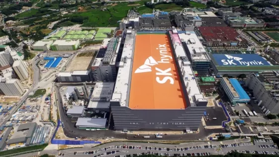
Memory chip vendor SK Hynix is considering a move into 2.5D chip packaging as a foundry outsource operation, according to South Korea’s ETnews.
The move may be partially driven by SK Hynix’s sub-ordinate role to foundry TSMC in the creation of AI accelerators for Nvidia. If SK Hynix could offer 2.5D packaging skills it could potentially offer to work in parallel with TSMC and perform the integration of GPU die and high-bandwidth memory (HBM) DRAM components in AI acceleration components.
To read the full article, click here
Related Chiplet
- DPIQ Tx PICs
- IMDD Tx PICs
- Near-Packaged Optics (NPO) Chiplet Solution
- High Performance Droplet
- Interconnect Chiplet
Related News
- SK hynix Signs Investment Agreement of Advanced Chip Packaging with Indiana
- SK hynix Signs Preliminary Memorandum of Terms with U.S. Department of Commerce for Advanced Packaging Facility in Indiana
- 2.5D/3D chip technology to advance semiconductor packaging
- 2.5D Integration: Big Chip Or Small PCB?
Latest News
- AI Optical Interconnect Boom Drives U.S. Firms to Expand Southeast Asia Outsourcing, Opening the Door for Cross-Industry Entrants
- GlobalFoundries accelerates adoption of co-packaged optics for advanced AI data centers with SCALE optical module solution
- TSMC SoIC roadmap targets 2029 chip stacking
- Applied Materials Broadens Advanced Packaging Portfolio with Acquisition of NEXX
- AI Competition Turns into a Supply Chain Arms Race, Tightening Advanced Packaging and 3nm Capacity