NanoIC opens access to first-ever fine-pitch RDL and D2W hybrid bonding interconnect PDKs
New advanced interconnect PDKs pave the way for high‑density, energy‑efficient chip‑to‑chip integration.
LEUVEN (Belgium), MARCH 2, 2026 — Today, the NanoIC pilot line, a European initiative coordinated by imec and dedicated to accelerating innovation in chip technologies beyond 2nm, releases two first-of-a-kind advanced interconnect process design kits (PDKs): a fine-pitch redistribution layer (RDL) and die-to-wafer (D2W) hybrid bonding PDK. These early-access PDKs bring advanced packaging capabilities within reach of universities, start‑ups, and industry innovators and mark an important step in enabling high‑density, energy‑efficient chip‑to‑chip connectivity.
As the semiconductor industry moves toward ever more complex and heterogeneous system architectures, advanced packaging has become a key enabler in supporting this progress. Instead of merely enclosing individual chips, today’s packaging technologies bring multiple dies (chiplets) together into tightly integrated systems where performance, energy efficiency, and bandwidth hinge on how effectively those components can interact. By enabling chiplets to be interconnected at high density, advanced packaging provides the foundation for the next generation of high‑performance computing, AI accelerators, and data‑intensive applications.
To enable universities, start‑ups, SMEs, and industrial players to turn these concepts into practical designs, NanoIC today releases the first version of its fine-pitch redistribution layer (RDL) and die‑to‑wafer (D2W) hybrid bonding process design kits (PDKs). These PDKs, built on the NanoIC pilot line, give designers early access to the design rules and validated building blocks needed to explore high‑density chip‑to‑chip integration.
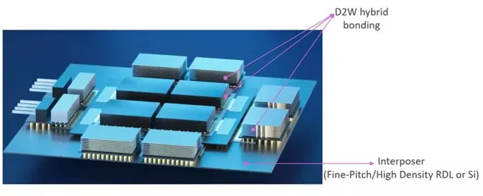
Fine‑pitch RDL PDK: high‑density routing on polymer‑based substrates
The fine‑pitch redistribution layer (RDL) PDKintroduces a new way to achieve high‑density chip‑to‑chip connections using polymer‑based substrates. Traditionally, these substrates could not support extremely fine lines, limiting their use in advanced packaging. Imec’s technology, developed within the NanoIC project, overcomes this barrier by enabling exceptionally small‑pitch interconnects in a polymer‑based RDL, offering capabilities that go beyond what leading commercial fabs provide today. With line widths and spaces down to 1.3 microns and microbump pitches as tight as 20 microns, the RDL PDK gives designers access to interconnects that can improve communication speed by up to 40% and reduce energy per bit by as much as 15%, on a UCIe-Advanced die-to-die interface. As a result, fine‑pitch RDL becomes an appealing integration option for a wide range of emerging applications, from automotive and high‑performance computing to next‑generation GPU architectures.
D2W hybrid bonding PDK: ultra‑dense die‑to‑die 3D connections
D2W hybrid bonding adds a second powerful integration technique by enabling extremely compact, direct connections between dies using the third dimension. Instead of relying on traditional copper bumps, hybrid bonding forms direct oxide‑to‑oxide links between the CMOS die and the package interface. This eliminates the parasitics associated with copper bumping and enables low‑loss, energy‑efficient communication pathways.
With its ability to create ultra‑dense, high‑bandwidth chip‑to‑chip links, the D2W hybrid bonding PDK is particularly suited for AI applications, advanced computing platforms, and high‑performance GPU architectures.
An important step toward full tape-out capabilities
With this release, imec becomes the world’s first to offer easy‑access interconnect PDKs at these integration levels and dimensions. This initial “exploratory version” provides the essential tools designers need to begin assessing the technology: systematic layout creation, automated and custom routing, and design rule checks.
“This first release is a pathfinding PDK,” Nicolas Pantano, head of the demonstrator architect team at imec, explains. “It gives researchers, start‑ups, and companies the essential tools to start designing, testing ideas, and providing feedback. As the PDKs mature, they will grow from exploratory design kits into complete, fabrication‑ready toolsets with tape‑out capabilities, enabling designers to take a layout created with these PDKs and have it physically manufactured on the pilot line, validating their concepts in silicon, not just in simulation.”
With the launch of these two interconnect PDKs, NanoIC expands its offering to a total of five publicly accessible process design kits. Following earlier releases of the N2, A14, and eDRAM PDK, the introduction of the fine‑pitch RDL and D2W hybrid bonding PDKs marks the next milestone in building a complete beyond‑2nm design toolkit, spanning logic, memory, and now also interconnect technologies. To support hands‑on exploration, NanoIC also hosts a dedicated workshop on the RDL and D2W PDKs on May 27, 2026. All practical details are available on the NanoIC website.
This work has been enabled in part by the NanoIC pilot line. The acquisition and operation are jointly funded by the Chips Joint Undertaking, through the European Union’s Digital Europe (101183266) and Horizon Europe programs (101183277), as well as by the participating states Belgium (Flanders), France, Germany, Finland, Ireland and Romania. For more information, visit nanoic-project.eu.
Related Chiplet
- DPIQ Tx PICs
- IMDD Tx PICs
- Near-Packaged Optics (NPO) Chiplet Solution
- High Performance Droplet
- Interconnect Chiplet
Related News
- Imec demonstrates die-to-wafer hybrid bonding with a Cu interconnect pad pitch of 2µm
- Adeia Demonstrates Hybrid Bonding Technology During Chiplet Summit 2024
- Adeia Presents Metrology Techniques for Improved Yield in Hybrid Bonding at IMAPS Device Packaging Conference 2024
- SEMI 3D & Systems Summit to Spotlight Trends in Hybrid Bonding, Chiplet Design and Environmental Sustainability
Latest News
- AI Optical Interconnect Boom Drives U.S. Firms to Expand Southeast Asia Outsourcing, Opening the Door for Cross-Industry Entrants
- GlobalFoundries accelerates adoption of co-packaged optics for advanced AI data centers with SCALE optical module solution
- TSMC SoIC roadmap targets 2029 chip stacking
- Applied Materials Broadens Advanced Packaging Portfolio with Acquisition of NEXX
- AI Competition Turns into a Supply Chain Arms Race, Tightening Advanced Packaging and 3nm Capacity