Hybrid Bonding Comes of Age Slowly and Collectively
Presentations at this year’s IEEE Hybrid Bonding Symposium showed how hybrid bonding is transitioning from lab demonstrations to industrial reality—exposing new challenges in testing, CMP control, and die-to-wafer integration.
By Pat Brans, EE Times | January 26, 2026
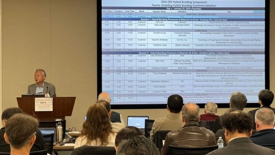
When the IEEE Hybrid Bonding Symposium convened in Silicon Valley on Jan. 22 and 23, it did so with a noticeably broader and more industrially grounded agenda than its inaugural edition a year earlier. Hosted by SEMI International, the second annual event reflected a technology that is no longer confined to a narrow set of image sensor or memory applications but is steadily pushing toward mainstream heterogeneous integration—albeit with significant hurdles still to clear.
The 2026 program spanned materials science, surface chemistry, process integration, metrology, inspection, reliability, testing, and yield modeling. Taken together, the abstracts underscored how hybrid bonding has become a deeply interdisciplinary challenge. Papers explored sub-micron copper-to-copper bonding physics, dielectric surface preparation, chemical-mechanical planarization (CMP) control, stress and warpage, advanced X-ray and acoustic inspection, AI-assisted defect detection, and even digital-twin modeling of bond interfaces.
The breadth of topics signaled both progress and fragility: Hybrid bonding is advancing rapidly in pitch and performance, but its success increasingly depends on tight coordination across the entire process flow—from design through test and inspection—rather than on any single breakthrough.
To read the full article, click here
Related Chiplet
- DPIQ Tx PICs
- IMDD Tx PICs
- Near-Packaged Optics (NPO) Chiplet Solution
- High Performance Droplet
- Interconnect Chiplet
Related News
- Adeia Demonstrates Hybrid Bonding Technology During Chiplet Summit 2024
- Adeia Presents Metrology Techniques for Improved Yield in Hybrid Bonding at IMAPS Device Packaging Conference 2024
- SEMI 3D & Systems Summit to Spotlight Trends in Hybrid Bonding, Chiplet Design and Environmental Sustainability
- EV Group Hybrid Bonding, Maskless Lithography and Layer Transfer Solutions for Heterogeneous Integration to be Highlighted at ECTC 2024
Latest News
- AI Optical Interconnect Boom Drives U.S. Firms to Expand Southeast Asia Outsourcing, Opening the Door for Cross-Industry Entrants
- GlobalFoundries accelerates adoption of co-packaged optics for advanced AI data centers with SCALE optical module solution
- TSMC SoIC roadmap targets 2029 chip stacking
- Applied Materials Broadens Advanced Packaging Portfolio with Acquisition of NEXX
- AI Competition Turns into a Supply Chain Arms Race, Tightening Advanced Packaging and 3nm Capacity