How the Worlds of Chiplets and Packaging Intertwine
By Majeed Ahmad, EETimes (September 26, 2023)
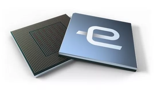
Chiplets mark a new era of semiconductor innovation, and packaging is an intrinsic part of this ambitious design undertaking. However, while chiplet and packaging technologies work hand in hand to redefine the possibilities of chip integration, this technological tie-up isn’t that simple and straightforward.
In chip packaging, the bare chip die is encapsulated in a supporting case with electrical contacts. The case protects the bare die from physical harm and corrosion and connects the chip to a PCB. This form of chip packaging has existed for decades.
To read the full article, click here
Related Chiplet
- DPIQ Tx PICs
- IMDD Tx PICs
- Near-Packaged Optics (NPO) Chiplet Solution
- High Performance Droplet
- Interconnect Chiplet
Related News
- ISE Labs Investment Secures the Establishment of New Site for Semiconductor Packaging and Test in Mexico
- The Evolution of Interconnects in Microelectronics Packaging
- The Role of Chiplets in Redefining Semiconductor Design
- DreamBig Semiconductor Announces Partnership with Samsung Foundry to Launch Chiplets for World Leading MARS Chiplet Platform on 4nm FinFET Process Technology Featuring 3D HBM Integration to Solve Scale-up and Scale-out Limitations of AI for the Masses
Latest News
- Xanadu and EV Group partner to build industrial-scale photonic quantum hardware
- AI Optical Interconnect Boom Drives U.S. Firms to Expand Southeast Asia Outsourcing, Opening the Door for Cross-Industry Entrants
- GlobalFoundries accelerates adoption of co-packaged optics for advanced AI data centers with SCALE optical module solution
- TSMC SoIC roadmap targets 2029 chip stacking
- Applied Materials Broadens Advanced Packaging Portfolio with Acquisition of NEXX