Chiplets 101: An Arteris Guide to Multi-Die Architecture

The semiconductor industry is entering a new phase of system design, where performance, power, and scalability are no longer dictated solely by transistor density, but by how effectively data moves through increasingly complex architectures.
 Chiplets and multi-die systems have emerged as a practical response to the slowing of Moore’s Law, the processing demands of artificial intelligence (AI), and the growing physical constraints of advanced process nodes.
By breaking down large monolithic systems-on-chip (SoCs) into smaller, functionally specialized dies, chiplets offer a path to improved yield, increased performance, and greater flexibility and scalable system integration.
Chiplets provide a path forward by enabling systems to scale beyond the limits of a single die, but they also introduce a new level of architectural complexity. And while designing with chiplets is an architectural transformation, success depends on how well designers can partition systems, manage communication between dies, and maintain performance predictability across distributed silicon.
This guide explains why chiplets matter, how multi-die systems work, and what it takes to design them successfully. It frames chiplets not as a packaging solution but as a system-architecture challenge centered on data movement, interconnect, and scalability.
What Is a Chiplet?
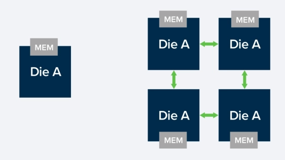
A chiplet is a modular silicon die, or building block, designed to perform a specific function, such as compute, memory, or I/O. Chiplets interoperate within a package as a large system-on-chip (SoC) to manage complex workloads across devices and applications, including AI and ML.
For instance, instead of a single monolithic die, compute may reside on one chiplet, with memory on another, and I/O or accelerators on additional dies. These chiplets are connected through high-speed die-to-die interfaces, forming a complete system with the following key characteristics:
- Modularity: Each chiplet serves a defined purpose
- Reusability: Chiplets can be reused across products
- Heterogeneity: Different chiplets can use different process nodes
- Interoperability: Standardized interfaces enable integration
In effect, chiplets transform SoC design into system integration at the package level, thereby improving yield, increasing flexibility, and reducing production costs.
Why Chiplets, Why Now?
For decades, semiconductor progress followed a predictable path: integrate more functionality into a single die, shrink transistors, and increase performance. That path is coming to an end.
Moore’s Law is no longer keeping pace with the demands of modern compute. While transistor scaling once doubled performance every two years, AI workloads are now increasing compute requirements on a much shorter cadence.
At the same time, physical constraints are becoming more pronounced. Reticle limits cap the size of a single die, and yield decreases as die size increases. Meanwhile, the cost of advanced nodes continues to rise, making large monolithic designs economically challenging.
Chiplets offer an alternative path. Instead of forcing all functionality into a single die, designers can partition systems across multiple smaller dies, each optimized for its role. These dies are then integrated at the package level to form a complete system.
Rather than eliminating complexity, the chiplet approach redistributes it. The challenge moves from manufacturing a single piece of silicon to architecting a distributed system of interconnected dies.
What Makes a Chiplet Different?
A chiplet is more than just a smaller chip. It is a modular, reusable silicon building block designed to operate within a larger system.
Unlike traditional SoCs, chiplets must communicate across die boundaries. This introduces new considerations around latency, bandwidth, and power that must be addressed at the architectural level.
Why do Chiplets Matter?
Chiplets improve yield, enable heterogeneous integration, and allow systems to scale beyond reticle limits. They also support reuse, enabling faster development and more flexible product strategies across markets and applications.
What are the Benefits of Chiplets?
Chiplets fundamentally change how semiconductor systems are built, offering significant benefits around performance, scalability, cost efficiency, portfolio flexibility, and ecosystem enablement. These benefits include:
- Improved performance as different functions can be built on the most appropriate node.
- Increased scalability by allowing systems to grow horizontally beyond the size limitations of a single die.
- Improved cost efficiency because smaller dies are easier to manufacture and test, resulting in an improved yield during manufacturing.
- Growing portfolio flexibility from the ability to mix and match chiplets to create differentiated products.
- Support for multi-vendor ecosystems through standardized interfaces and reusable chiplets.
However, these benefits are not automatic. They are the result of deliberate architectural decisions. Designing a chiplet-based system requires understanding how functionality is partitioned, how data flows between dies, and how performance is maintained across the entire system.
In this sense, chiplets represent a shift from integration to composition. Designers are no longer simply building chips but assembling systems.
Understanding Chiplet System Complexity
Not all chiplet systems are created equal. The complexity of a multi-die system increases significantly as it evolves from homogeneous configurations to heterogeneous, ecosystem-driven architectures.
Early chiplet designs often consist of identical dies arranged in fixed topologies. These systems are relatively straightforward to design and optimize. As systems become more heterogeneous, incorporating different types of chiplets with varying functions, the complexity increases. Communication patterns become less predictable, and integration challenges grow.
The ultimate vision of chiplets is an open ecosystem where chiplets from different vendors can interoperate seamlessly. While this model offers tremendous flexibility, it introduces significant challenges in standardization, verification, and system integration.
What is an Interconnect in Multi-Die Systems?
In a multi-die system, the interconnect is the communication fabric that enables data to move between chiplets as if they were part of a unified system. It spans both on-die networks (such as a NoC) and die-to-die links, bridging separate pieces of silicon across package-level interfaces.
Unlike monolithic SoCs, where communication is relatively short-range and tightly controlled, a multi-die interconnect must manage longer distances with higher latency sensitivity, and significantly more complex traffic patterns. It is responsible not only for transporting data, but for maintaining ordering, enforcing coherence when required, and ensuring predictable performance under load.
As a result, the interconnect is no longer just a wiring mechanism, but becomes the architectural backbone of the system, determining how efficiently compute resources can access data and ultimately, how the entire multi-die system performs.
Interconnect: The Defining Element
In multi-die systems, the interconnect transforms from a supporting component to the defining element of system performance, with coherent and non-coherent die-to-die communication, serving different use cases.
- Non-coherent communication is typically used for simpler data transfers and is simpler.
- Coherent communication enables shared memory models and is essential for high-performance computing and AI workloads. However, it introduces significant architectural complexity, particularly in maintaining consistency across multiple dies.
The interconnect must deliver high bandwidth, low latency, and power efficiency while operating across physical boundaries. Achieving this balance requires careful architectural planning, as poor interconnect design can lead to bottlenecks that negate the benefits of chiplet-based scaling. As a result, the interconnect becomes a primary design consideration rather than just an implementation detail.
Chiplet Topology and System Behavior
The arrangement of chiplets within a system, known as the topology, directly impacts performance, power, and scalability, and is a foundational decision that shapes system behavior. There is a wide range of possible topologies, from simple point-to-point connections to more complex mesh and hierarchical structures, and each topology presents tradeoffs.
Fully connected systems minimize latency but increase complexity and power consumption. Mesh networks provide scalability but can introduce congestion. Hub-and-spoke configurations simplify routing but may create bottlenecks at central nodes.
Selecting the appropriate topology requires understanding the system’s communication patterns. Workloads that require frequent data exchange between chiplets may benefit from low-latency, high-connectivity topologies, while others may prioritize efficiency and simplicity.
Why Memory Architecture is Important
In chiplet-based systems, the memory architecture is no longer uniform or implicit; it is explicitly managed and optimized. Multi-die systems introduce non-uniform memory access (NUMA), where memory access latency depends on the location of the data relative to the requesting compute element.
Each chiplet maintains its own local address map, and memory accesses must be reinterpreted as they cross die boundaries, creating a hierarchy of memory access latencies. Local memory accesses are faster, while remote accesses incur additional delay. Managing these differences is critical for maintaining performance.
NUMA effects require coordination between hardware and software, so system architects must design memory hierarchies that minimize latency for critical operations. In contrast, software must be aware of data placement and access patterns.
The Role of Packaging for Chiplet Design Scale
Advanced packaging technologies, such as 2.5D interposers and 3D stacking, enable chiplet systems to scale beyond traditional limits. While interposer-based designs can support systems significantly larger than reticle-limited monolithic dies, packaging alone does not guarantee performance. Although it provides the physical means to connect multiple dies, it does not address the architectural challenges of data movement, latency, and power efficiency.
Designers must ensure that the system architecture fully leverages packaging capabilities, as without proper planning, the benefits of advanced packaging can be overshadowed by interconnect inefficiencies and system-level bottlenecks. In this sense, packaging is an enabler, but architecture determines the outcome.
The Challenges of Chiplet Interoperability
One of the most promising aspects of chiplets is the potential for open ecosystems, even while achieving true interoperability remains a challenge. Several obstacles remain, including variability in UCIe implementations, complexity in protocol standards such as AMBA CXS, and the lack of standardized discovery and addressing mechanisms.
Verification is another critical issue. Chiplets developed by different teams or vendors must be validated to work together reliably. This requires standardized verification methodologies and “golden” models that ensure compatibility across implementations.
Unless these challenges are addressed, chiplet ecosystems remain constrained, and interoperability is not just a technical problem, but a systemic one that requires coordination across the entire industry.
Why System Architecture is the Differentiator
In the era of chiplets, system architecture is the primary differentiator, with success depending on the ability to design systems that balance performance, power, and scalability, while managing the complexity of distributed silicon. This requires a holistic approach that considers partitioning, interconnect, topology, and memory architecture as interconnected elements.
Solutions that enable structured interconnect design and system-level modeling are critical to this process. They provide the framework needed to manage complexity and ensure predictable system behavior.
Ultimately, the value of a chiplet-based system is determined not by the number of dies it contains, but by how effectively those dies work together.
The Arteris Perspective
Arteris approaches multi-die architecture as a system-level challenge centered on data movement, not just connecting chiplets. Arteris solutions span both non-coherent and coherent interconnect, enabling communication across chiplets, while maintaining performance and scalability.
FlexNoC and FlexGen provide non-coherent connectivity for scalable data transport, while Ncore enables fully coherent communication across multiple dies. Integration technologies, such as Magillem, support system assembly and configuration.
However, the core value lies not in individual components, but in the ability to design and manage an interconnect as a system fabric. This enables predictable performance, efficient data movement, and scalable architectures across a wide range of applications.
Redefining SoC Design
Chiplets are not simply an extension of traditional SoC design. They redefine it.
As scaling challenges intensify and AI-driven workloads continue to push system requirements beyond the limits of monolithic silicon, the industry is moving toward inherently distributed architectures.
Chiplets make that transition possible, enabling systems to scale in ways that were previously constrained by physical and economic boundaries. But the real shift is in how systems are designed, not how they’re packaged.
Success in a multi-die world depends on the ability to architect systems holistically: to partition intelligently, to manage data movement efficiently, and to ensure predictable behavior across increasingly complex, distributed environments. And the interconnect is no longer a supporting element; it is the system.
The teams that succeed are those that embrace this shift early, designing with system architecture as the foundation rather than an afterthought, because the future of semiconductor innovation will not be defined by how much functionality fits on a single die, but by how effectively entire systems work together in data movement.
Chiplets Q&A
What problem do chiplets solve?
Chiplets address the physical and economic limits of monolithic SoC design. As reticle limits, yield challenges, and rising costs constrain large die development, chiplets enable systems to scale by distributing functionality across multiple smaller dies. This allows designers to optimize each function independently while continuing to increase overall system performance.
Are chiplets just about packaging?
No. While advanced packaging technologies enable chiplets at the physical level, the real challenge lies in the architecture. Chiplets shift complexity from manufacturing to system design, requiring careful planning of data movement, interconnect, memory access, and system behavior across multiple dies.
How do chiplets impact performance?
Chiplets can improve performance by enabling heterogeneous integration and optimized process node selection. However, performance gains depend heavily on how efficiently data moves between dies. Poor interconnect design can introduce latency and bottlenecks that offset the benefits of scaling.
What role does the interconnect play in chiplet systems?
The interconnect is the backbone of a chiplet-based system. It manages communication between dies, ensuring data is delivered with the required bandwidth, latency, and ordering. In many cases, interconnect design becomes the primary determinant of overall system performance and scalability.
What is the difference between coherent and non-coherent communication?
Non-coherent communication is simpler and used for straightforward data transfers. Coherent communication enables shared memory across dies, which is critical for high-performance and AI workloads, but adds significant complexity in maintaining data consistency across the system.
What is UCIe and why is it important?
UCIe (Universal Chiplet Interconnect Express) is an emerging industry standard for die-to-die communication. It aims to enable interoperability between chiplets from different vendors, helping to create open ecosystems. While promising, achieving full interoperability still requires alignment in protocols, verification, and system integration.
Do chiplets reduce cost?
They can. Smaller dies generally have better manufacturing yield and can be reused across multiple products, reducing development costs. However, these savings depend on effective system design, as increased architectural complexity can introduce new costs in integration and verification.
What makes chiplet design challenging?
The key challenges include partitioning functionality across dies, managing data movement, ensuring predictable latency, handling NUMA effects, and verifying interoperability between components. These challenges grow significantly as systems become more heterogeneous and ecosystem-driven.
How does memory architecture change with chiplets?
Memory becomes non-uniform. Access latency depends on where data resides relative to the requesting chiplet. This requires both hardware and software to manage data placement carefully to avoid performance penalties.
What determines success in chiplet-based systems?
Success depends on system architecture. The ability to design interconnect, topology, and memory as a cohesive system determines whether chiplets deliver on their promise of scalability, performance, and efficiency.
Related Chiplet
- DPIQ Tx PICs
- IMDD Tx PICs
- Near-Packaged Optics (NPO) Chiplet Solution
- High Performance Droplet
- Interconnect Chiplet
Related Blogs
- A Smarter Path To Chiplets Through An Enhanced Multi-Die Solution
- A Beginner’s Guide to Chiplets: 8 Best Practices for Multi-Die Designs
- A Guide to Building Chiplets Today While Shaping Tomorrow’s Standards
- Synopsys and Alchip Collaborate to Streamline the Path to Multi-die Success with Soft Chiplets
Latest Blogs
- Chiplets 101: An Arteris Guide to Multi-Die Architecture
- 2.5D + 3D = “3.5D”!
- Addressing AI and Advanced Packaging Challenges with Synopsys 3DIO PHY
- Ultra-high repeatability and ultra-low insertion loss wafer and die-level visible-range E-PIC device characterization using an MPI Corp. probe system, enabled by process optimization from Quantum Transistors
- The Changing ASICs Landscape: the Shift Toward Chip Disaggregation