PulseForge Achieves Breakthrough in Ultra-Thin Wafer Processing, Demonstrating Photonic Debonding at less than 10-micron (µm) Silicon
Advancement surpasses industry benchmarks from Intel (~19 µm), Infineon Technologies (~20 µm), and Resonac (~25 µm), achieved in active collaboration with a leading Korean memory manufacturer
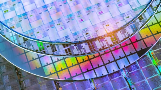
Austin, TX – April 13, 2026 – PulseForge, Inc., a leader in advanced electronics manufacturing solutions, today announced a major breakthrough in semiconductor manufacturing: successful photonic debonding of next-generation memory architectures fabricated on ultra-thin silicon wafers below 10 µm. This milestone was achieved in collaboration with a leading Korean memory manufacturer.
 This achievement builds on prior demonstrations with the same customer, where PulseForge enabled reliable debonding at less than 20 µm and 15 µm wafer thicknesses. The latest result at less than 10 µm represents a significant leap forward, addressing one of the most critical barriers in advanced semiconductor manufacturing: handling and debonding ultra-fragile wafers without compromising yield or device integrity.
As the semiconductor industry pushes toward thinner wafers to unlock performance and efficiency gains, PulseForge has now extended the frontier well beyond current published benchmarks:
- ~25 µm — Resonac (IEEE ECTC 2025 presentation) [1]
- ~20 µm — Infineon Technologies (press release by Infineon) [2]
- ~19 µm — Intel (press release by Intel) [3]
- ~8 µm — PulseForge (2026, latest demonstration)
Reducing wafer thickness is a key lever for performance. For example, thinning to ~20 µm has been shown to reduce substrate resistance by up to 50% and power losses by more than 15%. At the system level, these electrical improvements translate directly into more energy-efficient AI data centers—enabling lower power consumption per compute operation, improved thermal management, and higher performance per watt across large-scale GPU and HBM deployments. PulseForge’s demonstration at less than 10 µm pushes into a regime previously considered impractical due to extreme wafer fragility, warpage, and yield risks.
The ability to reliably debond at sub-10 µm thickness enables transformative advancements across multiple markets:
Advanced Memory (HBM, DRAM, NAND)
- Enables ultra-thin die stacking for next-generation HBM
- Increases bandwidth and improves thermal performance
- Supports scaling for AI and high-performance computing
Logic & Advanced Packaging
- Enables 3D integration, chiplets, and hybrid bonding
- Reduces interconnect length for improved latency and performance
- Supports wafer-to-wafer and die-to-wafer stacking
Power Semiconductors
- Reduces conduction losses and substrate resistance
- Enables thinner, higher-efficiency devices
- Supports electrification and AI data center power demands
PulseForge’s photonic debonding platform is uniquely suited for ultra-thin wafer processing at scale:
- Superior yield at extreme thinness
Non-contact, low-stress debonding process eliminates wafer breakage below 10 µm and preserves device integrity - Reusable LAL-coated carriers
Enables multiple reuse cycles, significantly lowering consumable cost and improving sustainability - Reduced cleaning requirements
Clean debond interface minimizes residue and simplifies post-process cleaning - Best-in-class cost of ownership (COO)
Fewer process steps, high throughput, reduced footprint, and lower consumables drive compelling economics
Additionally, the process is adhesive-agnostic, allowing seamless integration into existing semiconductor manufacturing flows.
PulseForge has demonstrated capability across an industry-leading range of material thicknesses:
- ~0.7 nm — 2D material / TMDC transfer (imec collaboration)
- Less than 10 µm — Silicon wafer debonding (latest milestone, advanced memory)
- Less than 20 and 15 µm — Memory architectures (customer validation)
This breadth—from atomic-scale materials to production-scale wafers—highlights the precision, scalability, and versatility of PulseForge’s platform.
“Our collaboration with a leading Korean memory manufacturer demonstrates that photonic debonding is not just viable—but essential—for enabling sub-10 micron wafer processing,” said Jonathan Gibson, CEO, PulseForge, Inc. He further added, “Our demonstration at ~8 microns establishes photonic debonding as a foundational technology for next-generation memory, logic, and power semiconductor manufacturing.”
With accelerating demand for AI infrastructure, high-bandwidth memory, and advanced packaging, photonic debonding is emerging as a foundational technology for the semiconductor industry:
- HBM scaling for AI compute
- 3D heterogeneous integration and chiplet architectures
- Energy-efficient power electronics for data centers
PulseForge is uniquely positioned to bridge the gap between material innovation and high-volume semiconductor manufacturing, enabling the next wave of AI-driven performance scaling.
References:
[1] https://ieeexplore.ieee.org/document/11038233
[2] https://www.infineon.com/regional/austria/press-release/2025/infineon-unveils-worlds-thinnest-silicon-power-wafer
[3] https://community.intel.com/t5/Blogs/Intel-Foundry/Systems-Foundry-for-the-AI-Era/Intel-Foundry-Achieves-Breakthrough-with-World-s-Thinnest-GaN/post/1743389
About PulseForge
PulseForge, Inc. develops and manufactures state-of-the-art flashlamp-based tools that deliver energy in a precise and targeted manner to enable innovation in industrial manufacturing. PulseForge’s expertise and tools empower customers to explore novel materials and manufacturing methodologies, driving dynamic and efficient production at an industrial scale.
Related Chiplet
- DPIQ Tx PICs
- IMDD Tx PICs
- Near-Packaged Optics (NPO) Chiplet Solution
- High Performance Droplet
- Interconnect Chiplet
Related News
- PulseForge Achieves Record Photonic Debonding Orders in Q1 2025, Signaling Market Acceleration
- Resonac and PulseForge Unite to Advance Photonic Debonding for Next-Gen Semiconductor Packaging
- PulseForge Announces Availability of PD700 SA – A Semi-Automated Photonic Debonding Tool Optimized for Large-Panel Advanced Packaging
- Global Zeus and PulseForge Introduce Fully-Automated Photonic Debonder
Latest News
- The Thermal Mismatch Problem Constraining Large-Format AI Chips Has Been Solved: ACCM's Celeritas HM50 & HM001 Address Warpage, Package Bow, and Signal Loss
- PacTech Launches Scalable Modular Wet-Bench System for Advanced Semiconductor Packaging
- PulseForge Achieves Breakthrough in Ultra-Thin Wafer Processing, Demonstrating Photonic Debonding at less than 10-micron (µm) Silicon
- Credo Agrees to Acquire DustPhotonics, Accelerating Expansion into Silicon Photonics and Next Generation Optical Connectivity
- Rapidus Opens Analysis Center and Rapidus Chiplet Solutions