The Future of Chip Integration: Fraunhofer IPMS Develops High-Density Chiplet Systems at the Wafer Level
May 19, 2026 -- Breakthrough in chip manufacturing: As part of the European APECS pilot line, researchers at Fraunhofer Institute for Photonic Microsystems IPMS have developed a method that allows different chip components to be fused almost seamlessly into a single unit. By precisely embedding small chiplets into specially structured silicon pockets, Fraunhofer IPMS succeeded in combining the advantages of a compact single chip with the flexibility of modular systems for the first time. This achievement demonstrates the feasibility of quasi-monolithic integration (QMI) and bridges the gap between traditional chip packaging and cutting-edge semiconductor manufacturing.
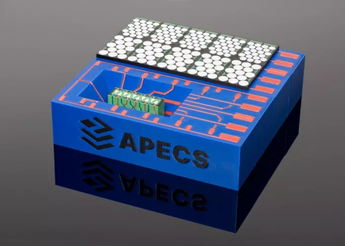
3D printing of a demonstrator for quasi-monolithic integration with a chiplet in the pocket.
Growing demands for greater complexity, computing power and system compactness are calling for a radical rethink of semiconductor manufacturing. The vision for future-proof microelectronics is to create systems that are as powerful as a single chip yet offer the flexibility of modular building blocks. Within the APECS pilot line, which focuses on "Advanced Packaging and Heterogeneous Integration for Electronic Components and Systems", Fraunhofer IPMS is pursuing the quasi-monolithic integration (QMI) approach. The aim is to integrate various chip components, such as control electronics, sensors and microelectromechanical systems (MEMS), at the wafer level, while retaining the benefits of a compact single chip.
From Theory to Reality: Pockets, Placement and Embedding
Researchers at Fraunhofer IPMS have successfully achieved the first critical milestone of the QMI roadmap. "The basis of QMI is silicon wafers with structured recesses, or pockets. For the first time, dummy chiplets have been inserted into these pocket wafers and the surface has been levelled with a passivation layer in preparation for subsequent back-end-of-line wiring," explains Dr. Lukas Lorenz, group leader at Fraunhofer IPMS. "This creates a nearly monolithic system architecture that combines the highest integration density with modular scalability." This success paves the way for the industrial maturity of the entire process chain for future applications.
Technological advantages: Higher system performance with maximum compactness
QMI technology offers significant advantages over conventional packaging processes. This is due to the way chiplets are arranged on an active or passive wafer substrate with a shared interconnect stack. Since the interconnects are formed in the front-end-of-line process, much higher connection densities can be achieved than with traditional methods. The following benefits result:
- Higher performance: Shorter signal paths reduce losses and latency, thereby increasing processing speed at the system level.
- Reliability: Reducing mechanical interfaces increases the robustness and operational lifetime of the systems.
- Compactness: QMI saves a significant amount of space because the elements are integrated in a nearly monolithic fashion.
- Cost-efficiency: Combining modular chiplet approaches enables highly cost-effective integration, short innovation cycles, and high scalability.
These advantages make quasi-monolithic integration ideal for innovations such as highly integrated system-on-chip (SoC) solutions for artificial intelligence (AI) applications and high-bandwidth smart transceivers.
Next Steps Toward Industrial Deployment
Dr. Lukas Lorenz emphasizes: "Although the current demonstrator is based on dummy structures, the process chain can be transferred to real-world customer applications. This enables a scalable integration architecture for future heterogeneous system solutions." Fraunhofer IPMS is targeting industrial partners whose products could benefit from the integration of different high-density technologies. The approaches developed within the APECS framework form the basis for quickly transferring QMI to production-oriented manufacturing environments. Further information is available on the Fraunhofer IPMS website.
APECS receives funding from the Chips Joint Undertaking and from national grants in Belgium, Germany, Finland, France, Greece, Austria, Portugal, and Spain, as part of the "Chips for Europe" initiative. The total funding for the APECS pilot line is €730 million over four and a half years.
Related Chiplet
- DPIQ Tx PICs
- IMDD Tx PICs
- Near-Packaged Optics (NPO) Chiplet Solution
- High Performance Droplet
- Interconnect Chiplet
Related News
- YES RapidCure Systems chosen by SkyWater Technology for Fan Out Wafer Level Packaging
- EV Group and Fraunhofer IZM-ASSID Expand Partnership in Wafer Bonding for Quantum Computing Applications
- European Chiplet Innovation: APECS Pilot Line starts Operation in the Framework of the EU Chips Act
- Fraunhofer IZM is powering the evolution of chiplet technologies as part of the APECS pilot line
Latest News
- The Future of Chip Integration: Fraunhofer IPMS Develops High-Density Chiplet Systems at the Wafer Level
- POET Technologies and Lumilens Advance Wafer-Level Photonic Integration for Next-Generation AI Optical Networks
- Tower Semiconductor Signs Customer Contracts for $1.3 Billion Silicon Photonics Revenue for 2027
- IC-Link by imec joins TSMC 3DFabric® Alliance to accelerate advanced packaging and 3D IC innovation
- EXTOLL announces Availability of Industry's first 16G UCIe PHY IP in GlobalFoundries 22FDX/22FDX+ Ready for Customer Integration