3D-IC in AI, HPC, and 5G: Bandwidth, Latency, and Energy per Bit Advantages
3D-IC technology is rapidly becoming the backbone of next-generation compute systems as traditional 2D scaling reaches physical and economic limits. Momentum is accelerating across industry, propelled by high-bandwidth memory (HBM) stacking, hybrid bonding, and chiplet partitioning, which together deliver step-function gains in bandwidth, latency, energy per bit, and integration density. Industry projections indicate that the hybrid bonding market alone is projected to reach USD $23.3 billion by 2032 (CAGR 5.5% from 2026 – 2032), underscoring the scale of adoption underway. These advances are reshaping high-demand sectors, including AI acceleration, high-performance computing (HPC), 5G infrastructure, edge computing, and automotive electronics.
By placing memory closer to compute, shortening vertical interconnects, and enabling heterogeneous co-packaging across process nodes, 3D-IC technology unlocks performance benefits once achievable only through monolithic scaling. The result is a new system design paradigm—one where architects tightly couple compute, memory, and signal-processing elements into compact, thermally optimized clusters tailored to real workloads. This blog post examines how these advantages manifest across key verticals and how Cadence technologies help engineering teams achieve predictable system-level integration and signoff.
AI/HPC with HBM: Memory Proximity and Throughput
Modern AI and HPC workloads are primarily dominated by one bottleneck: the cost of data movement. Whether training multi-billion-parameter transformer models or running physics simulations, performance increasingly hinges on how quickly data can be supplied to compute engines.
This is where 3D-ICs fundamentally change the equation.
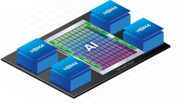
HBM + 3D-IC = A Vertical Highway for Data
Instead of routing memory traffic across DIMMs, sockets, and centimeters of PCB, 3D-ICs bring memory physically into the compute stack. HBM dies are vertically interconnected using through-silicon vias (TSVs) for vertical memory stacks or hybrid bonding for fine-pitch, low-parasitic die-to-die interfaces, forming thousands of parallel data channels only a few microns long.
This architectural shift delivers three transformative effects:
- Massive memory bandwidth: HBM3 and HBM3E provide 819GB/s to over 1TB/s per stack. With six to eight stacks mounted around the compute die, AI accelerators can sustain more than 6TB/s of architecturally provisioned bandwidth—enough to keep tensor cores saturated even during the most memory-intensive phases of training.
- Dramatically lower latency: When memory is physically adjacent to compute, signal flight time collapses. The propagation delay that once spanned a motherboard now shrinks to a vertical hop within the package. This latency reduction leads to more predictable model execution, faster convergence, and higher utilization in HPC pipelines.
- Lower energy-per-bit: Shorter interconnects require less drive strength, resulting in significant reductions in energy consumption. For hyperscale operators, where memory traffic is an essential contributor to power consumption, this improvement directly reduces operational costs and enhances sustainability metrics.
Cadence Advantage for AI/HPC
Cadence provides an architecture-to-signoff workflow that supports HBM-based stacks and tightly coupled AI accelerators:
- Integrity 3D-IC Platform for multi-die floorplanning, interposer routing, and pathfinding
- Clarity 3D Solver for accurate EM extraction of high-speed die-to-die links
- Celsius Thermal Solver for assessing stack thermals, gradients, and cooling feasibility
This integration helps teams evaluate bandwidth, thermals, and interconnect integrity early, long before physical design commits cost.
5G/Edge Compute: Latency and Integration Footprints
Ultra-low-latency signal processing and compact form factors are critical for 5G radios, edge inference modules, and multi-function edge systems.
Latency Reduction Through Near-Zero Interconnect Distance
3D-IC technology allows RF, AI accelerators, and baseband processing elements to be placed within microns of each other, where isolation and interference constraints allow, reducing:
- PHY-layer latency
- Parasitic inductance
- Timing variability in real-time control loops
Chiplet Partitioning for Multifunction Systems
3D-IC technology allows system designers to mix:
- RF/analog on mature nodes
- AI/ML accelerators on advanced nodes
- On-package memory
- High-density interposers
Cadence’s Allegro X Advanced Package Designer and Integrity 3D-IC Platform ensure die-aware and package-aware co-optimization for accurate system closure.
Automotive Compute: Reliability and Thermal Headroom
Automotive systems such as ADAS, autonomous driving, and zonal control require extreme reliability and predictable thermal behavior across long lifecycles.
Reliability Through Modular Chiplets
3D-IC technology supports:
- Known good die (KGD) assembly
- Stronger mechanical stability when combined with KGD strategies and robust mechanical design
- Greater resilience across temperature cycles and vibration
Thermal Feasibility Through Full-Stack Simulation
Stacked dies intensify power density, particularly in AI-driven workloads. Cadence’s Celsius Thermal Solver provides:
- Early thermal feasibility
- Gradient and coupling analysis
- Electro-thermal co-simulation with Clarity 3D Solver
- Hotspot prediction across stacks
These insights help ensure ISO 26262-aligned thermal reliability before design signoff.
Reference Architectures and Chiplet Partitioning Ideas
3D-IC technology enables new architectural patterns optimized for performance, power, and cost:
- Memory-on-logic (AI/HPC) with TSVs and hybrid bonding
- Logic + RF partitioning (5G/edge) across optimized nodes
- 2.5D silicon interposers for dense chiplet-to-chiplet routing
- UCIe-compatible ecosystems for interoperable chiplet reuse
Cadence’s Integrity 3D-IC Platform pathfinding evaluates TSV budgets, bump pitch, PDN feasibility, and stack-level behaviors early.
How to Evaluate Workloads for Stack Viability
Architects should assess:
- Bandwidth demands (AI training, HPC simulation)
- Latency sensitivity (beamforming, inference, radar/lidar)
- Thermal and power density of stacking
- Manufacturability and yield for TSV/pitch constraints
- Process-node flexibility and cost
Cadence’s Integrity 3D-IC Platform and Celsius Thermal Solver help determine whether a workload truly benefits from 3D integration.
3D-IC Is Redefining System Architecture Across Markets
As compute density increases and proximity-based processing becomes essential, 3D-IC technology is emerging as the defining architecture for AI factories, HPC clusters, 5G edge intelligence, and software-defined vehicles. With bandwidth exceeding a terabyte per second per stack, sub-10 µm hybrid bonding pitches, and maturing chiplet ecosystems, vertical integration is now surpassing the limits of planar scaling.
Cadence’s Integrity 3D-IC Platform, Clarity 3D Solver, Celsius Thermal Solver, and Allegro X Advanced Package Designer provide the unified, manufacturing-aware environment required to design, analyze, and sign off these advanced multi-die systems. Together, they equip engineering teams to deliver reliable, high-performance architectures that balance thermal efficiency, interconnect integrity, and manufacturability, setting the foundation for the next decade of intelligent computing.
Request a Design Assessment or Demo
If your team is exploring 3D-IC integration, you can request a design assessment to review stack feasibility, interposer requirements, and potential multiphysics risk areas. This collaborative evaluation helps identify where the Integrity 3D-IC Platform can improve integration efficiency, modeling accuracy, and time to signoff, giving your project a stronger foundation from the start.
- Explore the Cadence Multi-Die 3D-IC Solution to see how Cadence empowers next-generation system innovation.
- Explore the Integrity 3D-IC Platform to discover how 3D design and signoff enable system-level optimization.
- Explore the Allegro X Advanced Package Designer Platform to accelerate system performance and seamless integration.
- Explore how the Celsius Thermal Solver enables 3D-IC thermal planning and signoff.
- Talk to a 3D-IC Specialist to discuss your design challenges and roadmap.
Related Chiplet
- Interconnect Chiplet
- 12nm EURYTION RFK1 - UCIe SP based Ka-Ku Band Chiplet Transceiver
- Bridglets
- Automotive AI Accelerator
- Direct Chiplet Interface
Related Blogs
- Alphawave Semi Tapes Out Industry-First, Multi-Protocol I/O Connectivity Chiplet for HPC and AI Infrastructure
- Cadence Recognized for Accelerating AI and 3D-IC Applications by Samsung Foundry
- 3D-ICs in the Automotive Market: Breaking Barriers with AI-Driven EDA Tools
- Intel® Shows OCI Optical I/O Chiplet Co-packaged with CPU at OFC2024, Targeting Explosive AI Scaling
Latest Blogs
- 3D-IC in AI, HPC, and 5G: Bandwidth, Latency, and Energy per Bit Advantages
- Bosch and the chiplet revolution: Enabling software-defined mobility
- Addressing the Biggest Bottleneck in the AI Semiconductor Ecosystem
- Thermal Management in 3D-IC: Modeling Hotspots, Materials, & Cooling Strategies
- 3D Chips: Socionext Achieves Two Successful Tape-Outs in Just Seven Months