NHanced Semiconductors Leads the Semiconductor Industry in Heterogeneous Hybrid Bonding Production
The company’s recently delivered Besi Datacon 8800 CHAMEOultra plus system is the world’s first operational advanced bonder of its kind to enter production
MORRISVILLE, NC – December 16, 2025 – NHanced Semiconductors, the first U.S.-based pure-play advanced packaging foundry, uniquely supports mixed-material hybrid bonding with either copper or nickel bonds. Their new Besi bonding system further expands its advanced packaging yield and throughput.
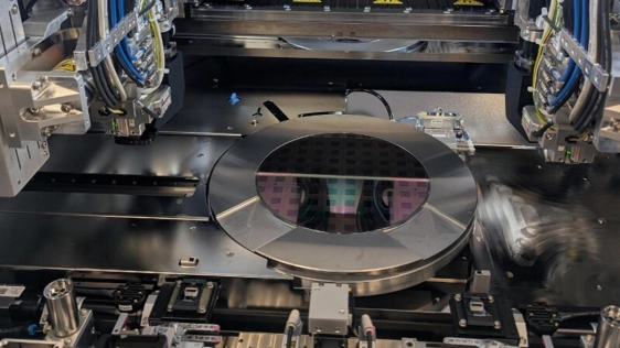 NHanced announced earlier this year that it had taken delivery of the first BE Semiconductor Industries (Besi) Datacon 8800 CHAMEOultra plus hybrid bonding system at the company’s advanced packaging facility in Morrisville, NC. The new bonding system represents the latest in ongoing investments by NHanced to expand its advanced packaging production. Among its suite of technologies, NHanced delivers the Direct Bond Interconnect (DBI®)† room temperature hybrid bonding process that joins wafers, dies, and chiplets with both dielectric covalent bonds and metal-to-metal fusion bonds. DBI® produces unmatched fine-grained interconnects for 2.5D and 3D assemblies. NHanced has uniquely expanded its DBI® process capabilities to include heterogeneous integration of GaN, GaAs, InP, LiNbO3, glass, and diamond substrates, and is the only company offering both copper and nickel for bonding.
“NHanced has already successfully delivered more hybrid bonding products than anyone else in the industry. The new Besi system significantly expands the hybrid bonding capabilities of our Morrisville, NC facility,” said NHanced president Robert Patti.
NHanced is the first pure-play advanced packaging foundry to operate this Besi hybrid bonding platform – a key enabler for ultra-precise die-to-wafer alignment of 200 nm with interconnect pitches down to 1 µm. The system can process up to 2,000 dies per hour, resulting in ~10x faster throughput with increased yields and superior warpage control.
NHanced has pioneered a paradigm shift in semiconductor manufacturing that it calls “Foundry 2.0” – applying semiconductor foundry processes and advanced packaging and assembly technologies to dies and chiplets sourced from traditional foundries. The results are customized 3DIC and 2.5D advanced packaging and interposer assemblies. NHanced is the only U.S.-based foundry that can support this manufacturing model.
About the Besi System
The Besi Datacon 8800 CHAMEOultra plus is an advanced hybrid bonding system that cost-effectively addresses increased demands for performance, speed, accuracy, and warpage control in fine-pitch copper interconnects with submicron pad sizes. Based on Besi’s field-proven Datacon platform, the Datacon 8800 CHAMEOultra plus hybrid bonder supports room temperature direct fusion bonding of dielectric followed by batch annealing to complete electrical connections and incorporates state-of-the art vision systems.
About NHanced Semiconductors, Inc.
Based in the US, NHanced Semiconductors is the world’s first pure-play advanced packaging foundry, specializing in leading-edge BEoL semiconductor technologies. Its capabilities include chiplets, 3D-ICs, silicon interposers, 2.5D, additive silicon manufacturing, photonics, microfluidics, and other innovative technologies. The foundry works with both standard and non-standard substrates, III‑V compound semiconductors, and many specialized materials.
Headquartered in Illinois, NHanced has a development and manufacturing facility near Research Triangle Park, NC, performing manufacturing, in-house process development, and customer prototyping, as well as a volume interposer and assembly facility in Odon, IN. For more information, please visit: https://nhanced-semi.com/
Related Chiplet
- Interconnect Chiplet
- 12nm EURYTION RFK1 - UCIe SP based Ka-Ku Band Chiplet Transceiver
- Bridglets
- Automotive AI Accelerator
- Direct Chiplet Interface
Related News
- NHanced Semiconductors Announces Delivery of the First Next-Generation Hybrid Bonding System from BE Semiconductor Industries
- EV Group Hybrid Bonding, Maskless Lithography and Layer Transfer Solutions for Heterogeneous Integration to be Highlighted at ECTC 2024
- EV Group Hybrid Bonding, Maskless Lithography and Layer Transfer Solutions for Heterogeneous Integration to be Highlighted at ECTC 2025
- OKI Develops Tiling crystal film bonding (CFB) Technology for Heterogeneous Integration of Optical Semiconductors onto 300 mm Silicon Wafers
Latest News
- NHanced Semiconductors Leads the Semiconductor Industry in Heterogeneous Hybrid Bonding Production
- PulseForge Announces Availability of PD700 SA – A Semi-Automated Photonic Debonding Tool Optimized for Large-Panel Advanced Packaging
- Global Semiconductor Equipment Sales Projected to Reach a Record of $156 Billion in 2027, SEMI Reports
- Strategic alignment between imec and Japan’s ASRA aims to harmonize standardization of automotive chiplet architectures
- TOPPAN to Install Pilot Line for Advanced Semiconductor Packaging at Ishikawa Plant